The key difference between PCBmodE and a traditional EDA is the ability to create patterns on the board in the different layers of the PCB using common graphics design tools. This allows for a greater amount of creativity in the layout phase of a design - at the expense of design rules that normal EDAs place to prevent you from doing the wrong thing.
PCBmodE is the creation of Dr. Saar Drimer from Boldport - an Electronics Craftmanship company which turns out some amazingly pretty and functional PCBs for a variety of clients.
So why did i not just use Kicad/Eagle/something else? Because i wanted to see what you can create using alternative tools and methodology from a regular board - and for the kicks.
First step was to design a circuit - for the project in mind i wanted something basic and obnoxious - so flashing LEDs it was.
Initially i was thinking of designing something with a basic clock and shifters - then came to my senses when i realised its cheaper now to buy a microcontroller then all the parts needed for an old 80's design.
I'd recently just come back from Defcon in the US and had lucky enough to get one of the badges DC503 made for their party ( designed by @securelyfitz ) which used the Atmel ATTINY85.
So i decided to rip their circuit off for this badge (sorry guys/girls)!
So i decided to rip their circuit off for this badge (sorry guys/girls)!
The Schematic
So i sat down and created a simple LED flasher circuit using charlieplexing to maximise the number of LEDs i could flash (again - wanting to annoying the maximum amount of people).
This uses a ATTINY85, a 5050 LED, a bunch of 1206 LEDs, 0805 resistors, a push button switch and a CR2032 coin cell battery
I ordered most of the components of Alibaba - my favourite place to buy components as it is cheap as chips - but slow, so slow.
Board Design
Next i had to design the board.
First step was to read the documentation and look at some of the example boards.
It took a while to grok how to design boards in PCBmodE.
Here's how i did it:
Here's how i did it:
Step 1 - Creation of Component Footprints
Create the component footprints in the ./components directory. I took the components json's given in the hello-solder project and then altered these to suit each component. The idea here was to get the components correctly defined before trying to get creative.
Step 2 - Placement of components
Place a few components in the ducksec-badge.json file to provide an idea of how it works.
Again here i took the hello-solder.json and stripped it down to suit my needs.
Again here i took the hello-solder.json and stripped it down to suit my needs.
Step 3 - Generate the SVG file
To generate the SVG from our test ducksec-badge.json we use the following command
python ../pcbmode.py -b ducksec-badge -m
from the ./cool-pcbs directory of PCBmodE
This generates an SVG file that i then open in Inkscape.
Shift-Ctrl-X gives you the XML description of the SVG.
So you select the outline layer
Click the unlock icon
Select the svg:path
Then copy the "d" values printed.
You then open the kiwicon-badge.json
Goto the "outline" tag
and insert the copied "d" values into the "value" string.
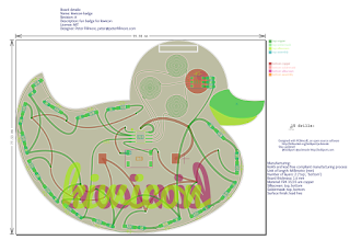
This generates an SVG file that i then open in Inkscape.
Step 4 - Creating the board outline
To form the shape of the board you edit the "outline" layer. Now this is not copied back to the JSON when you start editing so you have to copy theShift-Ctrl-X gives you the XML description of the SVG.
So you select the outline layer
Click the unlock icon
Select the svg:path
Then copy the "d" values printed.
You then open the kiwicon-badge.json
Goto the "outline" tag
and insert the copied "d" values into the "value" string.
"outline": {
"shape": {
"type": "path",
"value": "m 7.614166,...,-32.7480675 z",
"location": [
-0.1268844, -2.257778
]
}
},
Regenerate the board using the above PCBmodE command and you should see the shape you designed in Inkscape - here a nice rubber ducky.
Step 5 - Placing your components
Now you should be able to place your components on the board.
Here I created all the different components in the kiwicon-badge schematic and incremented the locations so they were spread around the generated SVG and I could clearly see them.
"D1": {
"footprint": "1206-LED",
"layer": "top",
"location": [
-6.9479856,
11.8223
],},
I then regenerated the SVG and start placing the components in the areas i want them on the board. To do this i lock all other layers and unlock the "assembly", "solderpaste", "soldermask", "silkscreen", "pads" and "drills" layers. Then select the whole component and place this where i want it.
After placing the components i can then regenerate the JSON file from my edited SVG using the following command:
So at this point you should be happy with the design you've made and almost ready for sending to your chosen board house.
To generate the gerber files:
The "--fab" argument allows you to set the files naming that a board manufacturer wants. In this case i used DirtyPCB; but you can adapt the pcbmode_config.json to suit the board house of your choice.
You can then review the generated gerbers using a gerber viewer to ensure that it looks correct on for each layer (personally i use gerbview included in the kicad package).
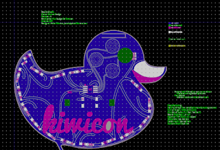
After placing the components i can then regenerate the JSON file from my edited SVG using the following command:
python ../pcbmode.py -b kiwicon-badge -e
This extracts your changes from the SVG and creates a JSON with them imbedded. Now this only works for certain layers - so you can't do this with the outline.Step 6 - Routing
Generate the SVG again with the changes you've made to date
python ../pcbmode.py -b kiwicon-badge -m
Select the "copper" folder and the "routing" layer.
Then start connecting the components together with curves in the SVG program. Take special care to not cross traces on a layer.
To add a via you draw a dot, then redefine that dot as a via in the XML of the SVG.
Take care in this step to slowly and methodically join the circuit together to match your schematic as you don't have a netlist to guide you.
Step 7 - Repeat steps 5 and 6
Iterate over steps 5 to 6 to design the board. Be artistic - this is why you are using PCBmodE!
Step 8 - Generate your gerbers/manufacturing files.
So at this point you should be happy with the design you've made and almost ready for sending to your chosen board house.To generate the gerber files:
python ../pcbmode.py -b kiwicon-badge --fab "dirtypcb"
The "--fab" argument allows you to set the files naming that a board manufacturer wants. In this case i used DirtyPCB; but you can adapt the pcbmode_config.json to suit the board house of your choice.
You can then review the generated gerbers using a gerber viewer to ensure that it looks correct on for each layer (personally i use gerbview included in the kicad package).

After
At this point i thought it looked good - so sent the board for printing.
I like dirtypcb as the shipping is cheap and quality is a lot higher then what they describe on the site.
I like dirtypcb as the shipping is cheap and quality is a lot higher then what they describe on the site.
A few weeks later i receive my boards and components needed. At this stage it was <1 week to kiwicon so i had to hope i hadn't mucked up and the circuit was good.
I threw one together in an hour or so and to my surprise all the parts worked;
except i had wired to the switch to the reset pin of the processor :(
And wired the switch closed :(
But easy to fix with a few bodge wires :)
except i had wired to the switch to the reset pin of the processor :(
And wired the switch closed :(
But easy to fix with a few bodge wires :)
Next i had to write some code - quick search got me a good avr-template and i was ready to roll.
PCB at:
https://github.com/peterfillmore/kiwicon_badge/pcbThings I broke in the rush
- Wired the switch to the reset pin of the microcontroller.
- Wired the switch closed.
- Didn't calculate idea resistors/currents for each LED (just threw them on the board and hoped)
- Burnt a few LEDs in assembly
- Disabled reset on a few ATTINYs and caused the chip to lose in circuit programming mode.
- Couldn't get interrupt on a remapped reset pin to work on the ATTINY
Other then that - it worked great.


No comments:
Post a Comment